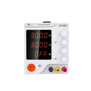
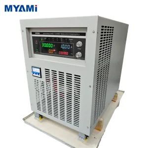
Explore our core engineering catalog featuring advanced DC-DC regulators, smart measurement units, and certified laboratory utilities.
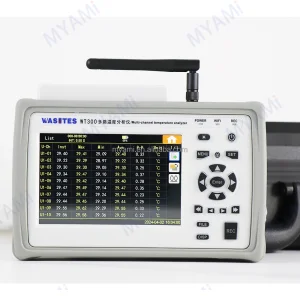

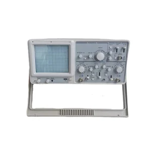
The global electronics landscape is shifting toward extreme specialization, particularly in high-power systems, automation, and green energy infrastructure. Underpinning this revolution is the requirement for high-reliability Custom OEM PCB Prototyping. High-reliability prototypes serve as the blueprint for volume manufacturing, validating mechanical tolerance, thermal performance, and signal integrity prior to commercial scale-up.
Procurement teams within global enterprises face critical challenges when choosing PCB prototype suppliers. They require partners capable of managing dense trace geometry, heavy copper configurations (ranging from 2oz to 6oz for power-carrying paths), and advanced base substrates (such as High-Tg FR-4, polyimide, and metal-core laminates). Standard run-of-the-mill services cannot accommodate the rigid testing guidelines and tolerances needed for industrial machinery and automotive components.
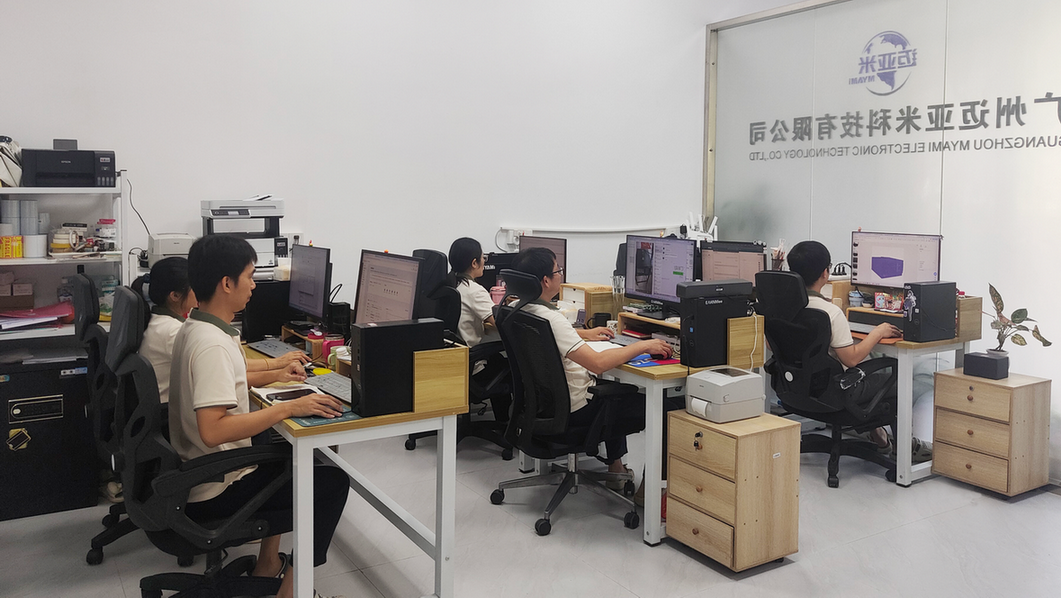
Headquartered in Shenzhen, China, Shenzhen Myami Power Technology Co., Ltd. (MYAMI) is a technology-driven manufacturer and solution provider specializing in high-precision, industrial-grade power supplies and electrical test equipment. Designed for engineering rigor, MYAMI bridges the gap between complex electronic research, high-voltage component testing, and scalable industrial automation.
By leveraging state-of-the-art diagnostic instruments, MYAMI continuously optimizes its own custom OEM PCB architectures. Power circuitry demands strict noise margin optimization, multi-phase thermal balancing, and highly responsive transient loops. This feedback loop between our proprietary testing equipment development and custom PCB fabrication enables us to deliver unmatched reliability for high-power, high-voltage applications.
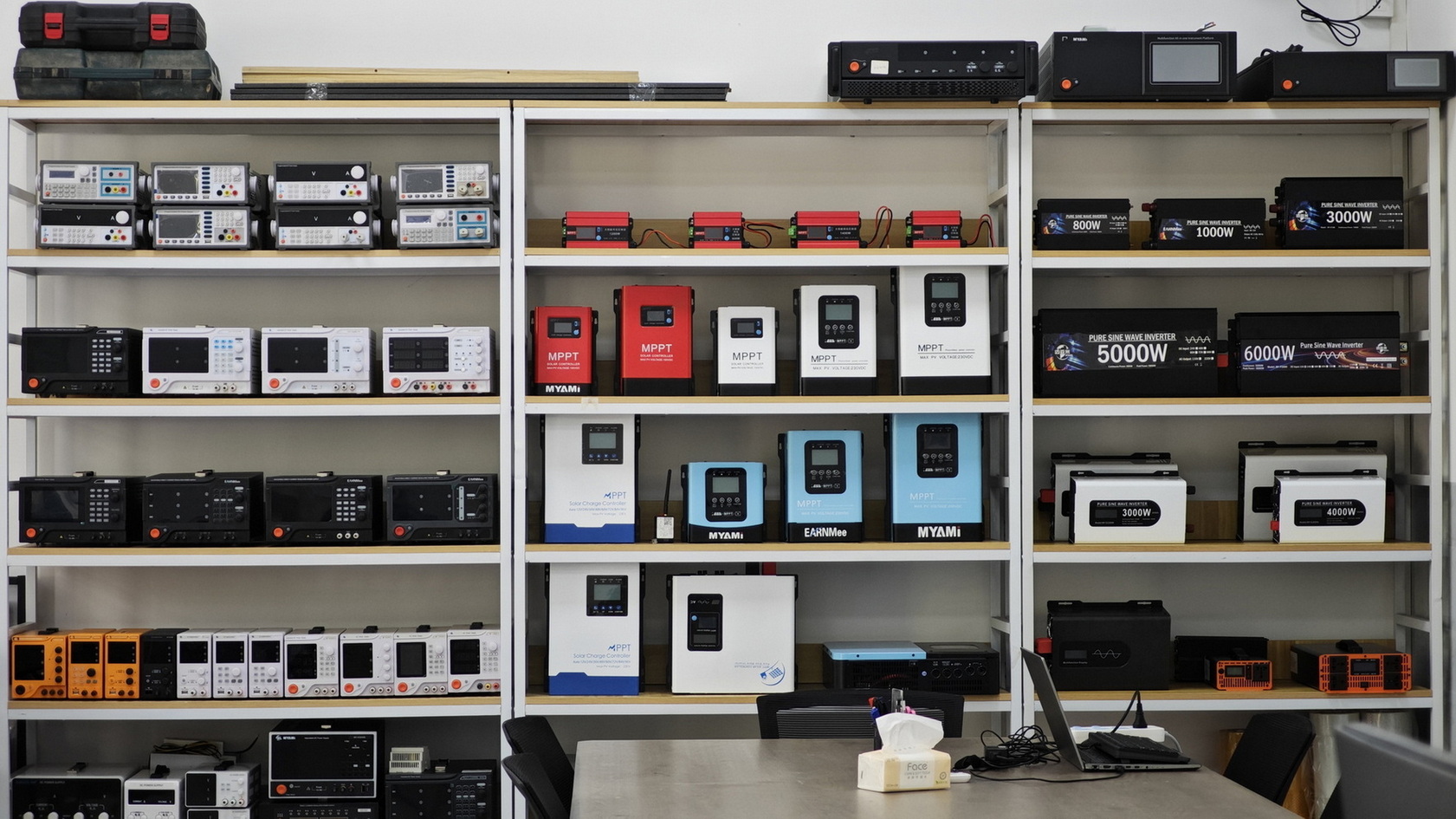
Delivering high-reliability testing systems and customizable component matrices for specialized industrial sectors.
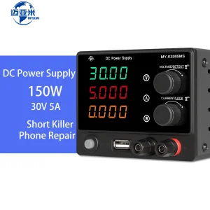
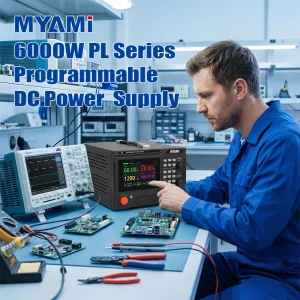
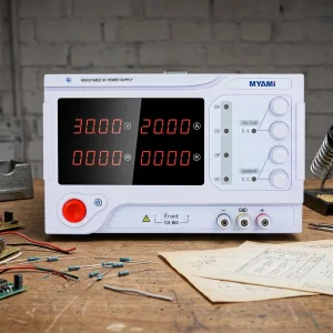
Featuring multi-digit LED displays, ultra-low ripple, and rapid transient response, engineered for precision electronic R&D, semiconductor evaluation, and PCB debugging.
Delivering high-current, high-voltage DC/AC regulated power supplies (ranging up to hundreds of volts and amperes) built for industrial motor drives, electroplating rectifiers, and heavy-duty component burn-in testing.
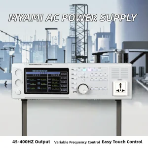
Providing specialized DC power units, battery simulators, and variable AC power sources engineered for Electric Vehicle (EV) On-Board Chargers (OBC), BMS evaluation, and solar inverter testing.
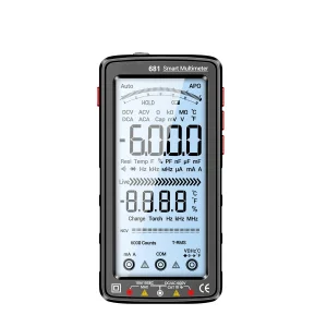
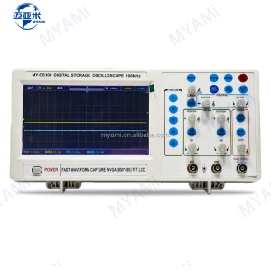
Supplying complementary test bench solutions, including digital oscilloscopes, multimeters, and specialized AC voltage regulators for global laboratories, space-agency simulation systems, and advanced academic technical institutes.
An end-to-end overview of our micro-assembly, PCB validation, and system integration workflows designed to satisfy international aerospace and consumer safety margins.
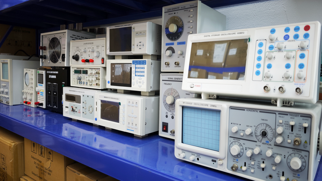
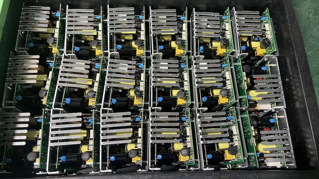
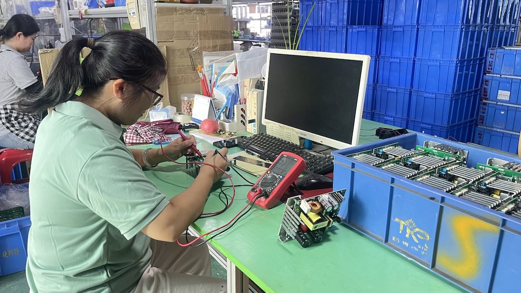
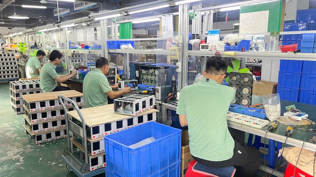
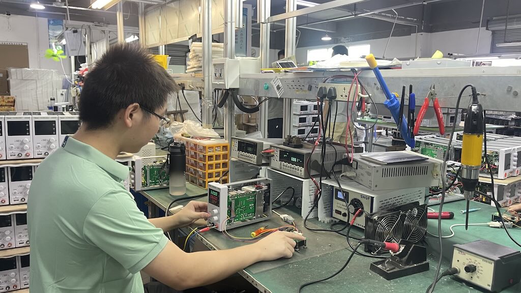
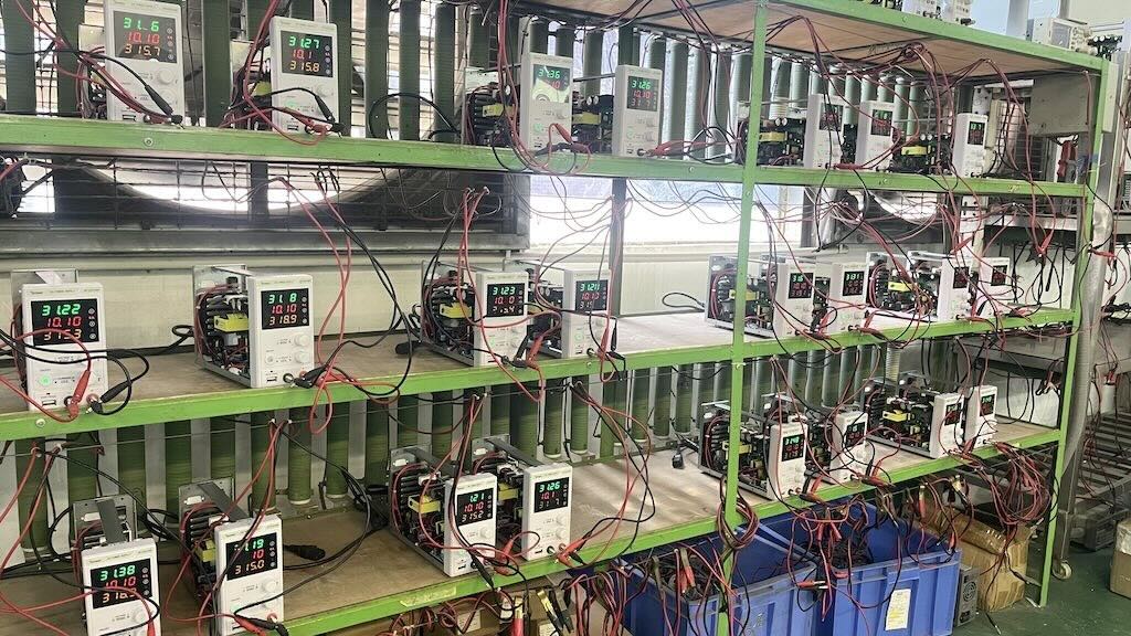
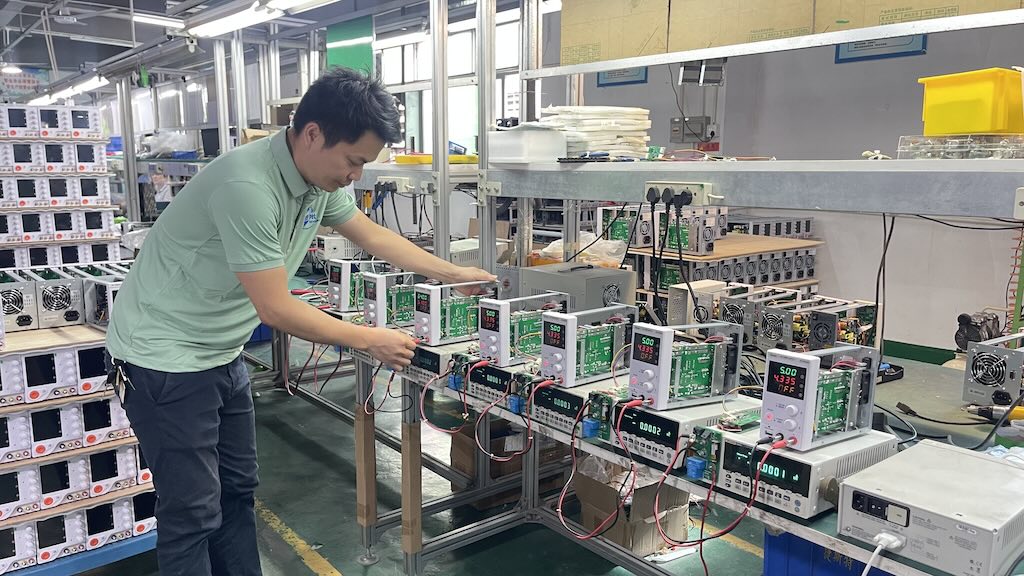
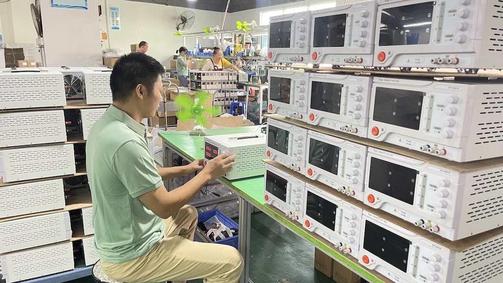
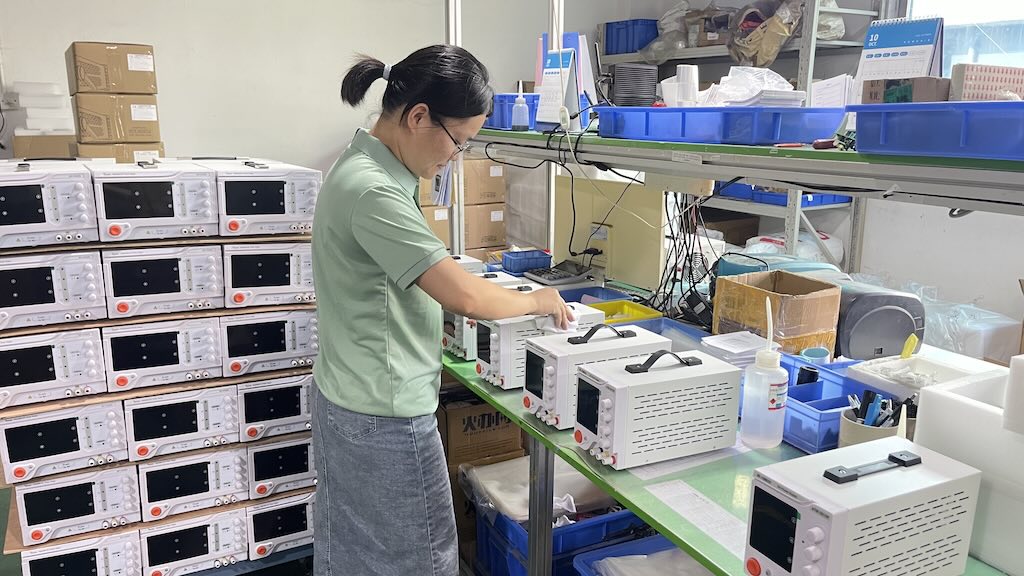
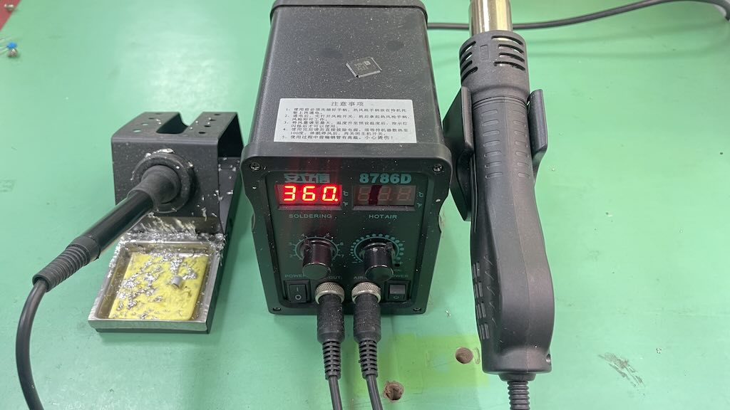
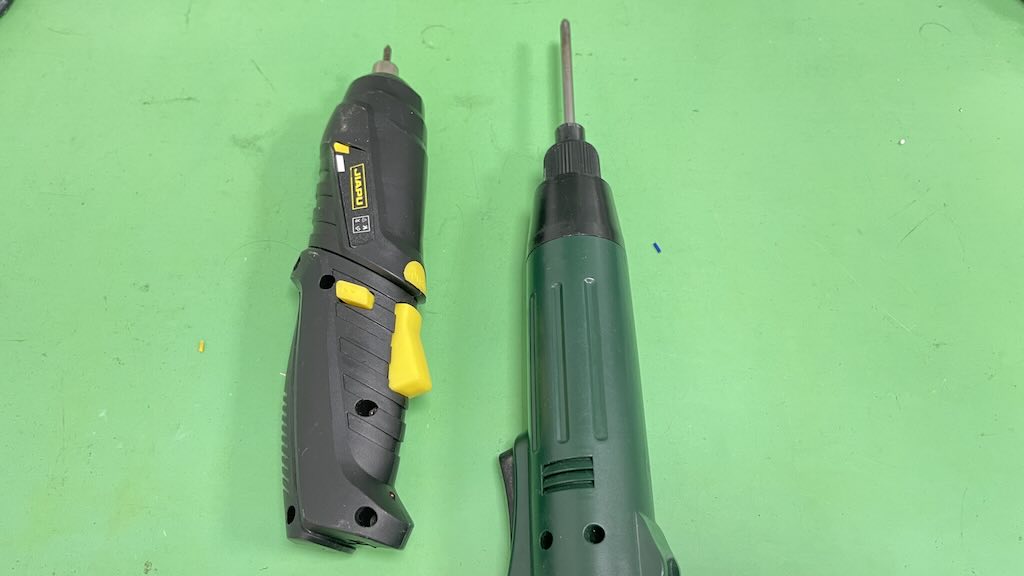
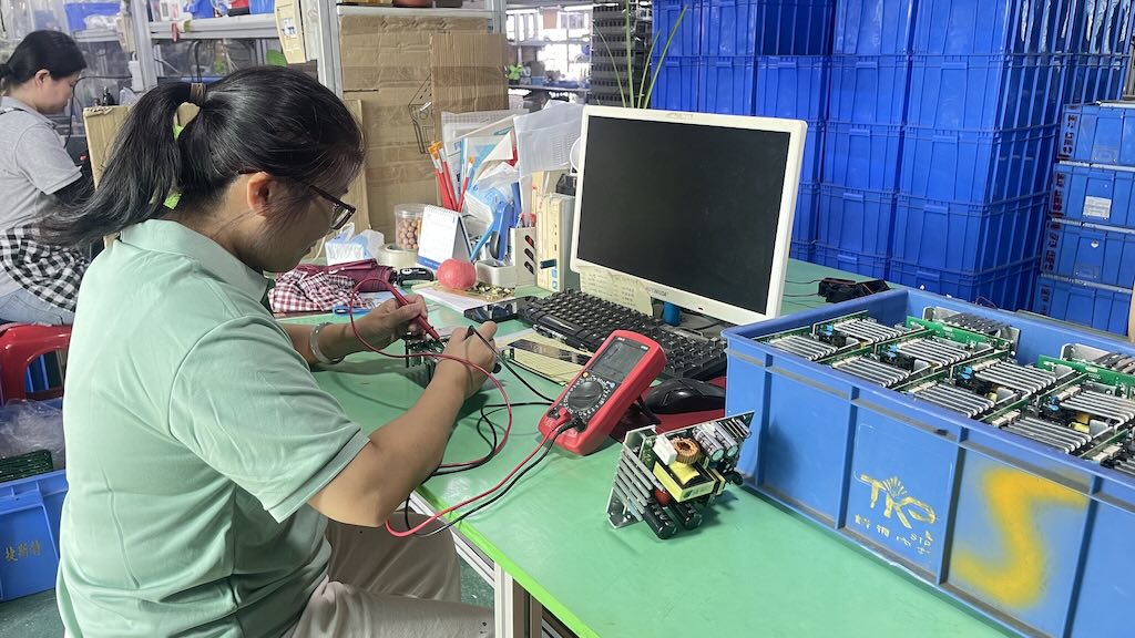
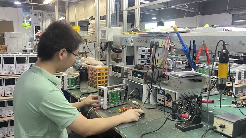
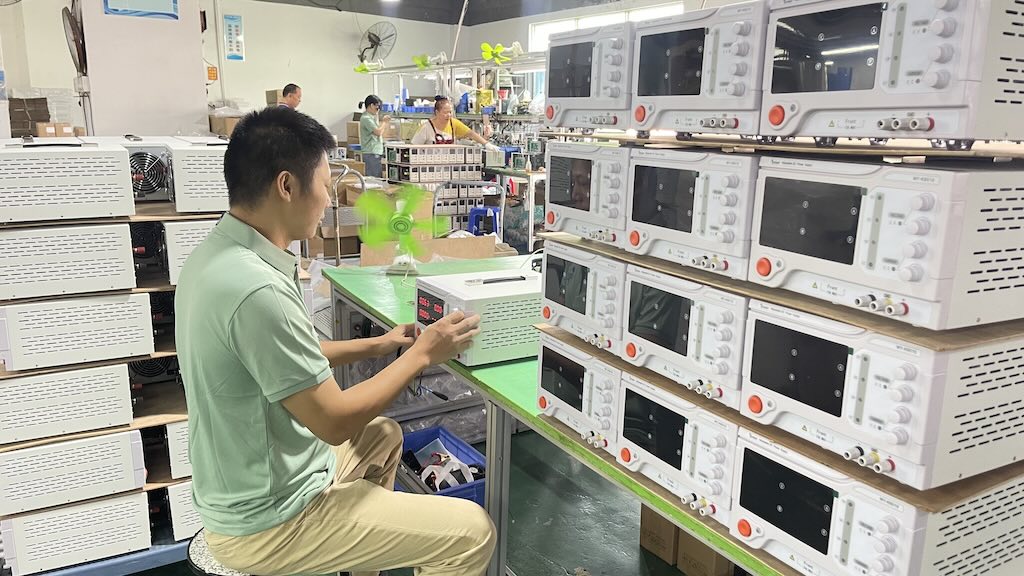
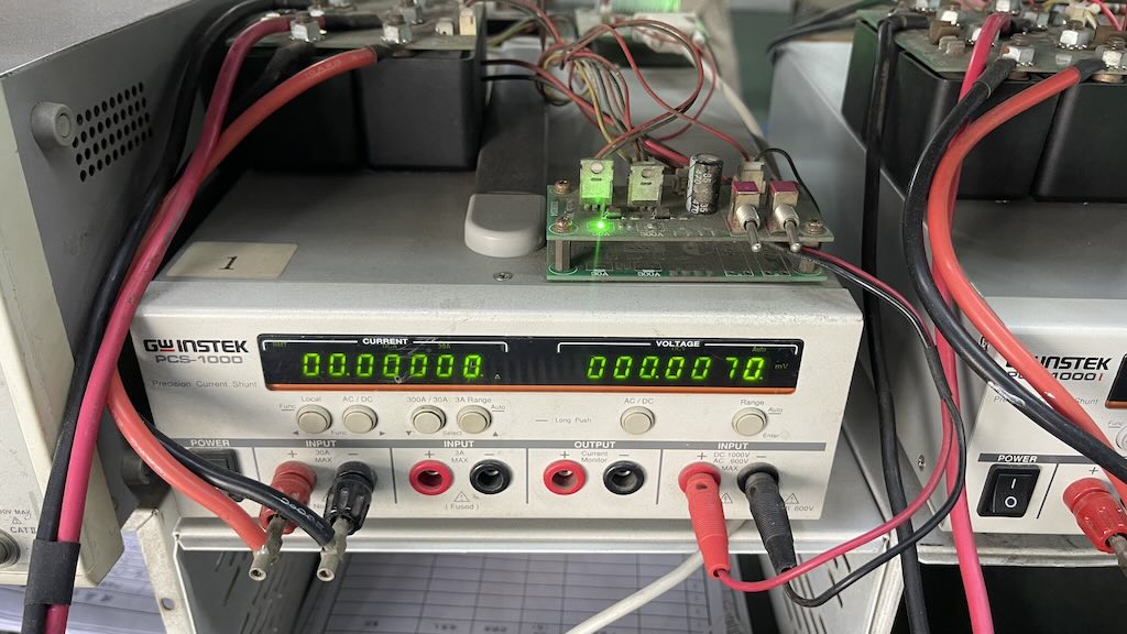
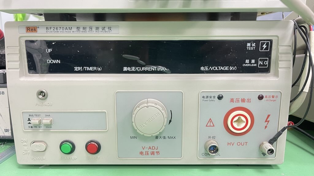
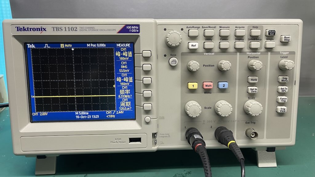
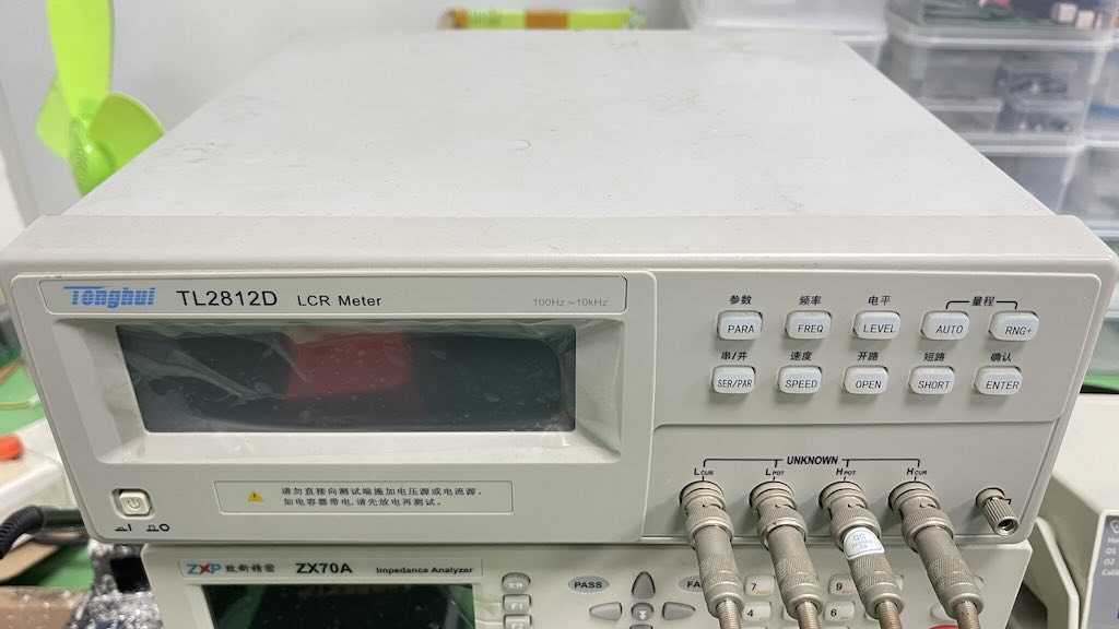
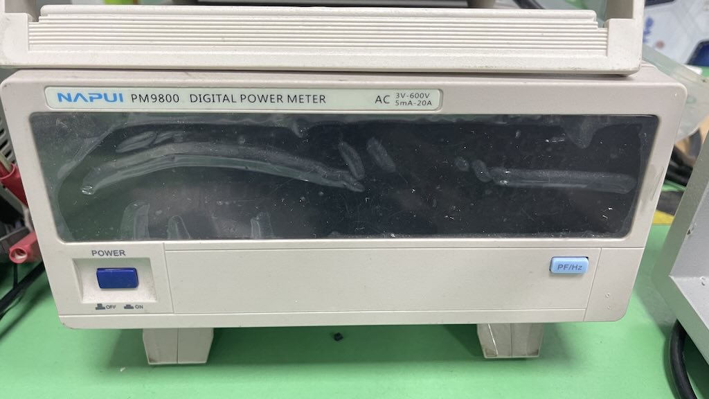
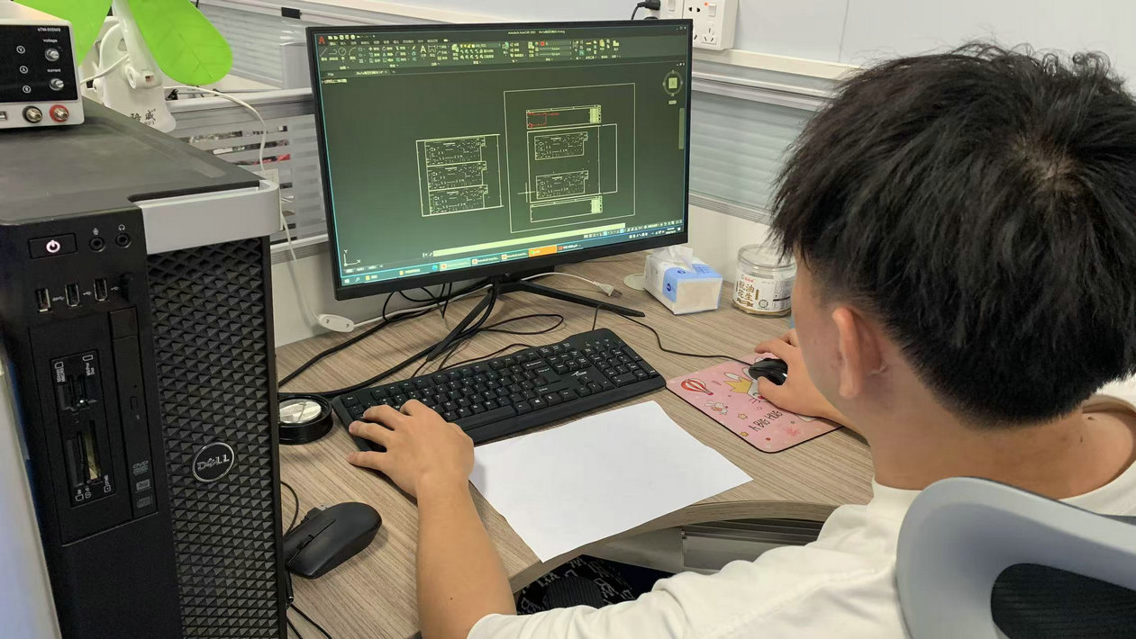
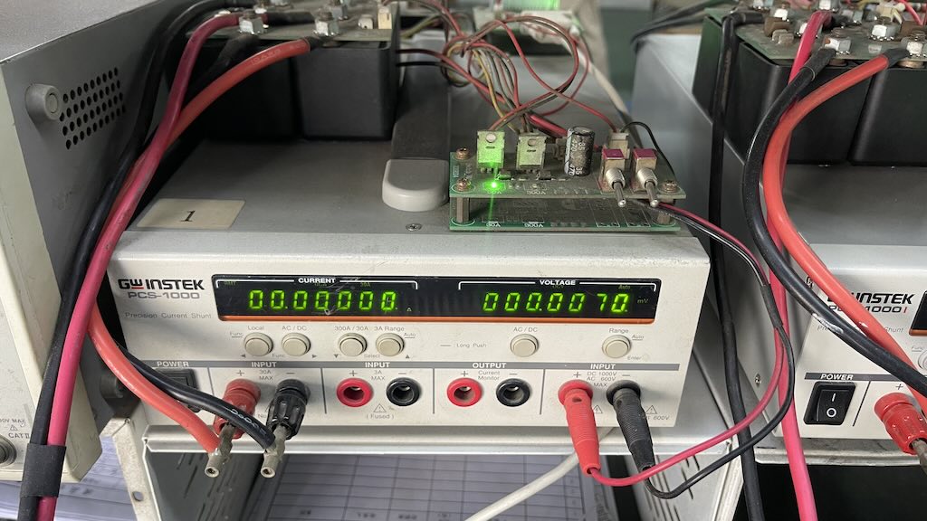
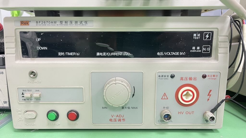
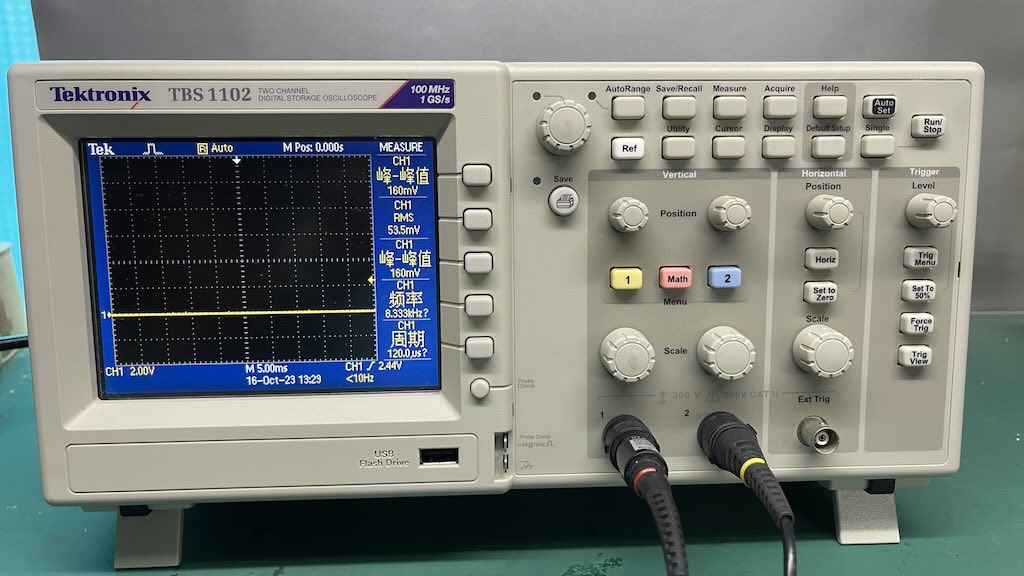
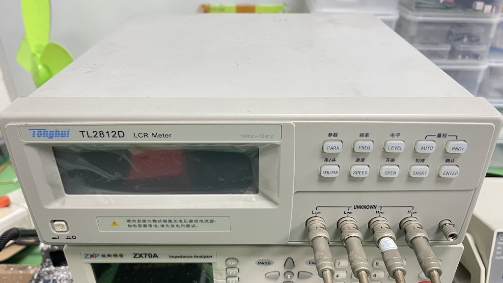
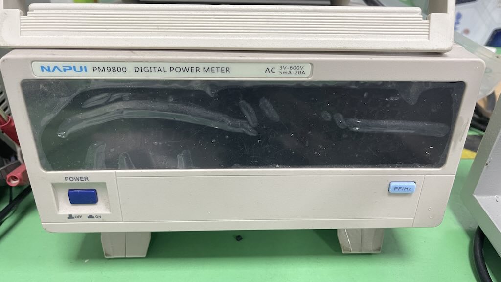
Providing the backbone of global electrical systems through specialized OEM capabilities and innovative topologies.
Standard circuit boards usually integrate 1oz (35µm) copper cladding. While sufficient for data lines and consumer-grade logic boards, this density fails when handling high current loads typical of high-performance variable frequency AC units or battery emulation stacks. At MYAMI, our design guidelines facilitate heavy copper traces up to 6oz, significantly minimizing thermal degradation, trace resistance, and electromagnetic interference.
Thermal management is key. By using multi-layer stack-ups, insulated metal substrates (IMS), and thermal vias filled with conductive epoxy, we ensure power components dissipate heat efficiently. This stabilizes transient states, increases operational lifespans, and maintains system calibration even under demanding industrial workloads.
MYAMI structures all multi-layer layouts under rigid electromagnetic compatibility (EMC) constraints. Signal degradation, loop area expansion, and parasitic capacitance are systematically controlled during the prototype design phase.
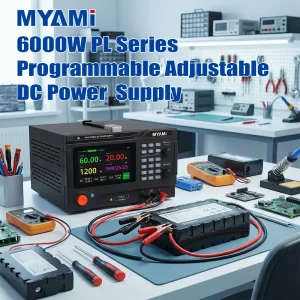
Each programmable diagnostic unit features comprehensive, layered protection arrays, including Over-Voltage Protection (OVP), Over-Current Protection (OCP), and Over-Temperature Protection (OTP). Integrated Modbus, CAN-Bus, and RS485 interfaces enable seamless connection to automated testing equipment (ATE) setups, preventing signal interference and providing clean power conversion metrics.
Validating On-Board Chargers (OBC), fast-charging battery packs, and vehicle-to-grid (V2G) power modules. Our high-voltage prototypes endure thermal cycle aging tests to withstand engine compartments and high-vibration automotive chassis.
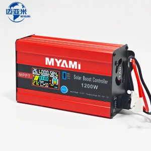
Optimizing efficiency in MPPT solar charge controllers and smart wind inverter interfaces. Our heavy-duty configurations process up to 1200W with 99% real-time tracking accuracy, reducing distribution losses.
Integrating telemetry modules, smart meters, and high-frequency power rails. Our PCBs support complex Modbus and Ethernet communication protocols, ensuring noise immunity in electromagnetically noisy factory environments.
Shipping high-power electronics and prototyping boards globally requires compliance with regional regulatory standards. Every PCB layout and device fabricated under the MYAMI umbrella meets strict international certifications:
By working with certified supply chain partners, we ensure that raw copper, FR-4 cores, and semiconductor components meet rigorous traceability standards.
We recognize that complex projects require close collaboration. With clients in North America, Europe, East Asia, and the Middle East, MYAMI provides comprehensive remote support, including raw CAD review, impedance matching analysis, and custom diagnostics.
Whether integrating RS485 communication protocols with your automated PLC lines or configuring high-voltage testing sources for aerospace simulations, our engineers provide detailed technical documentation and rapid-response remote support to streamline implementation.
Complete your deployment bench with high-capacity programmable power cabinets, variable AC sources, and diagnostic utilities.
Answering key technical questions regarding manufacturing capabilities, thermal management, and power diagnostics.
 Myami Power