Engineered for high stability, multi-layer circuit protection, and absolute calibration accuracy across complex test setups.


An Industry Whitepaper on Signal Integrity, Safety Certifications, and Global Testing Implementations
In the domain of modern electrical engineering, the accuracy of high-speed data acquisition is entirely contingent upon the physical interface connecting the unit under test (UUT) to the measurement analyzer. Oscilloscope probes serve as this critical bridge, acting not merely as physical cables, but as highly complex, balanced transmission networks. Operating under the strict mandates of the CE Certification (EN 61010-031 safety standard), manufacturers and suppliers must design these tools to prevent high-frequency signal degradation, loading errors, and user exposure to hazardous potentials.
E-E-A-T Technical Focus: A probe's electrical impedance must match the oscilloscope's analog front-end dynamically. At high frequencies, even minor inductive or capacitive variances translate directly into phase distortion and overshoot. Certified oscilloscope probes safeguard signal integrity, ensuring that what you measure matches the physical reality of the circuit.
CE marking verifies compliance with European safety regulations. For oscilloscope probes, this focuses on electrical shock prevention and transient overvoltage protection, categorized under Measurement Categories:
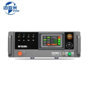
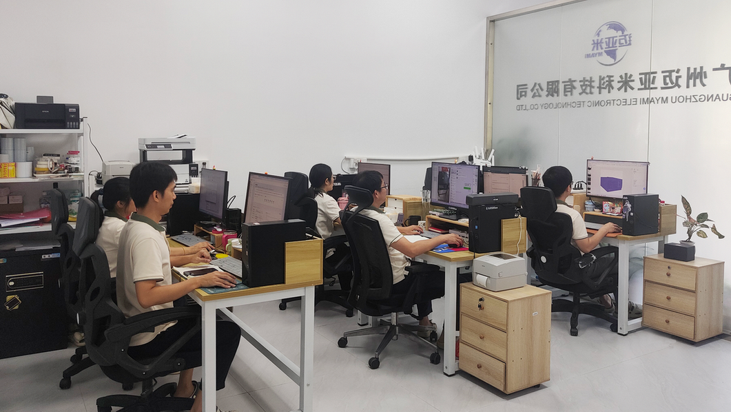
Headquartered in Shenzhen, China, Shenzhen Myami Power Technology Co., Ltd. (MYAMI) is a technology-driven manufacturer and solution provider specializing in high-precision, industrial-grade power supplies and electrical test equipment. Designed for engineering rigor, MYAMI bridges the gap between complex electronic research, high-voltage component testing, and scalable industrial automation.
Every MYAMI system is engineered with strict multi-layer protection protocols (OVP, OCP, OTP, and short-circuit safeguards) and complies with international safety and quality standards, including CE, RoHS, and ISO9001. Integrated with standard industrial control protocols (RS485, RS232, and CAN communication), our equipment seamlessly connects to automated production lines and central PC control systems.
Today, MYAMI serves research institutions, automotive OEMs, aerospace contractors, and electronics manufacturers across North America, Europe, East Asia, and the Middle East. Whether you require a single benchtop lab power supply or a custom high-power aging system, MYAMI is your ultimate partner for precision power and uncompromised testing reliability.
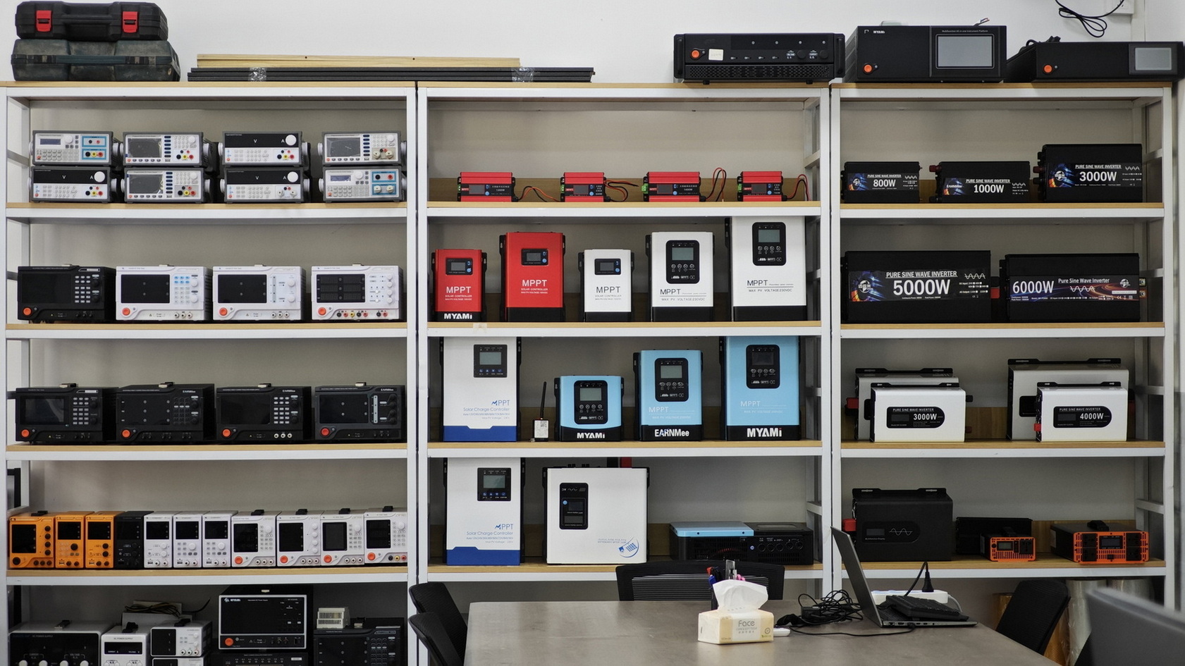
Four core operational pillars driving global R&D innovation, industrial diagnostics, and automated validation networks.
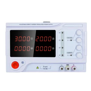
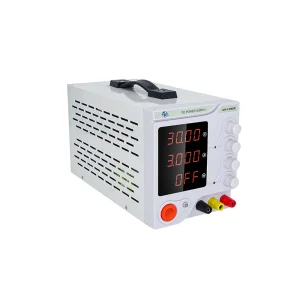
Featuring multi-digit LED displays, ultra-low ripple, and rapid transient response, engineered for precision electronic R&D, semiconductor evaluation, and PCB debugging.
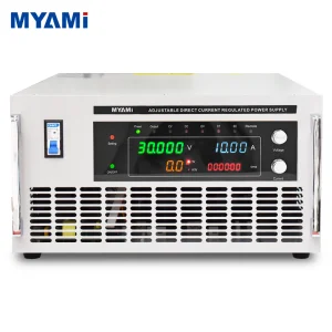
Delivering high-current, high-voltage DC/AC regulated power supplies (ranging up to hundreds of volts and amperes) built for industrial motor drives, electroplating rectifiers, and heavy-duty component burn-in testing.
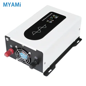
Providing specialized DC power units, battery simulators, and variable AC power sources engineered for Electric Vehicle (EV) On-Board Chargers (OBC), BMS evaluation, and solar inverter testing.
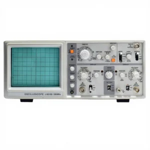
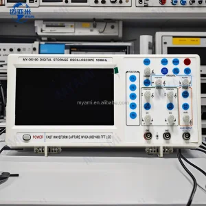
Supplying complementary test bench solutions, including digital oscilloscopes, multimeters, and specialized AC voltage regulators for global laboratories and technical institutes.
Inside the MYAMI Production Ecosystem: Vertical Integration, Rapid Prototyping, and Multi-Stage Validation Programs
Located in the heart of China’s electronic manufacturing hub, MYAMI harnesses a completely integrated supply chain network. From silicon sourcing to final calibration, our production systems maximize efficiency without compromising structural quality or component tolerances. Through vertical integration, we optimize raw materials routing, PCB layout check phases, structural assembly, safety calibration, and shipping logistics.
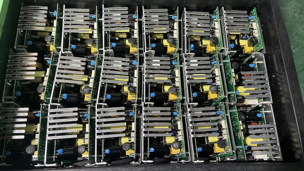 Raw Material
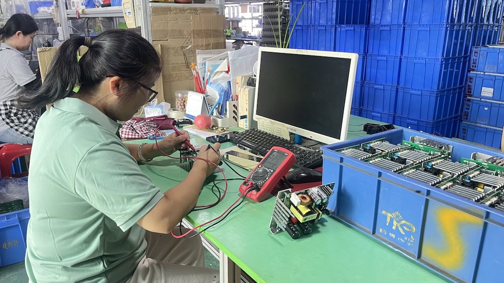 PCB Checking
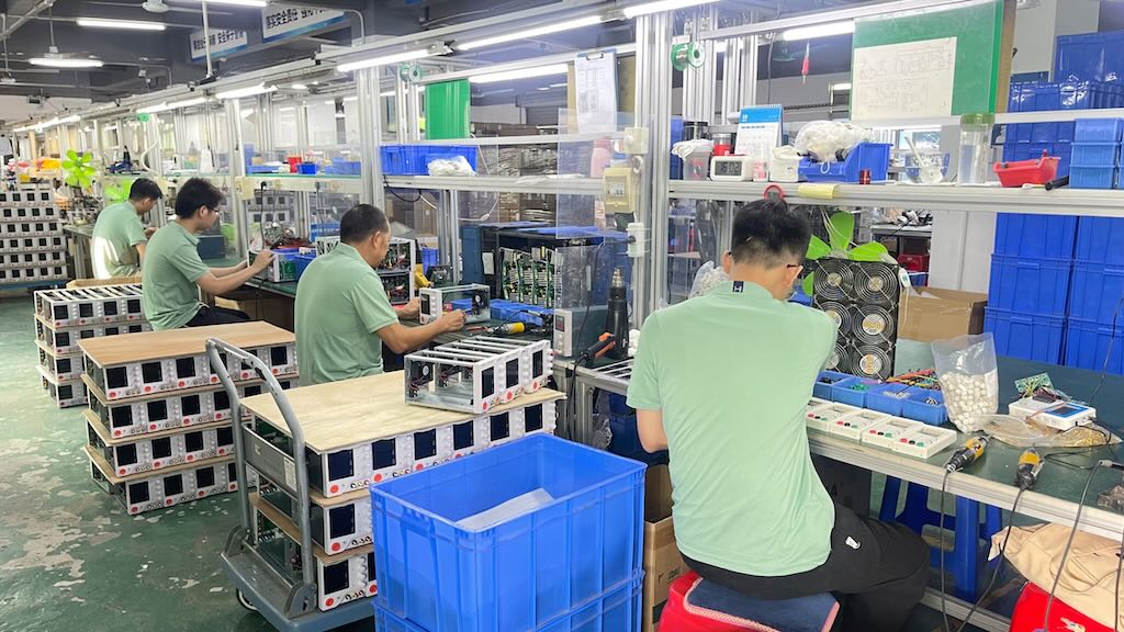 Assembling
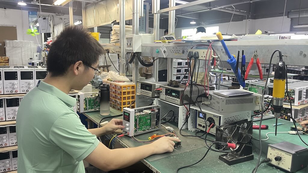 Debug
Debug
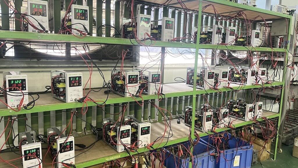 Aging
Aging
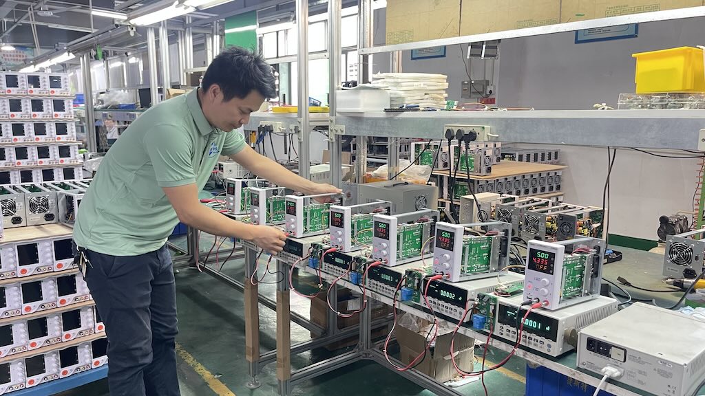 Calibration
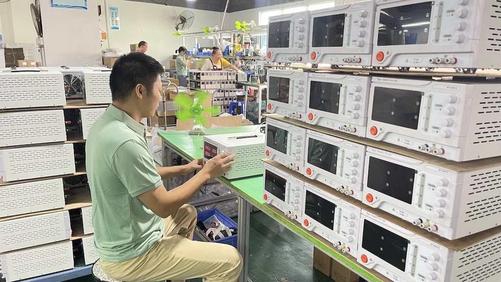 QC checking
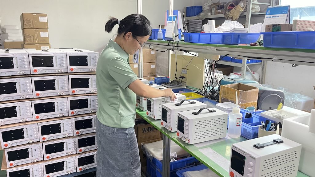 Packing
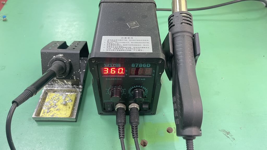 Soldering Station
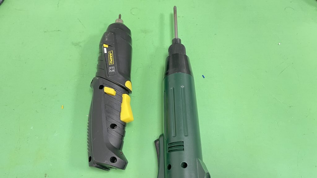 Electronic Screwdriver
How we utilize specialized test instrumentation to evaluate passive components, verify insulation safety, and ensure signal consistency.
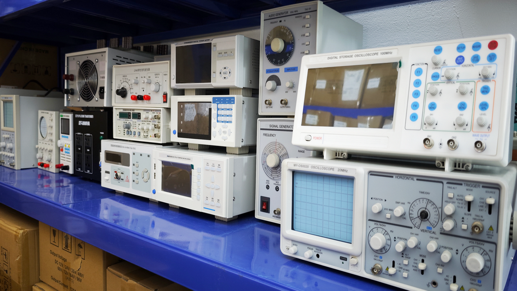
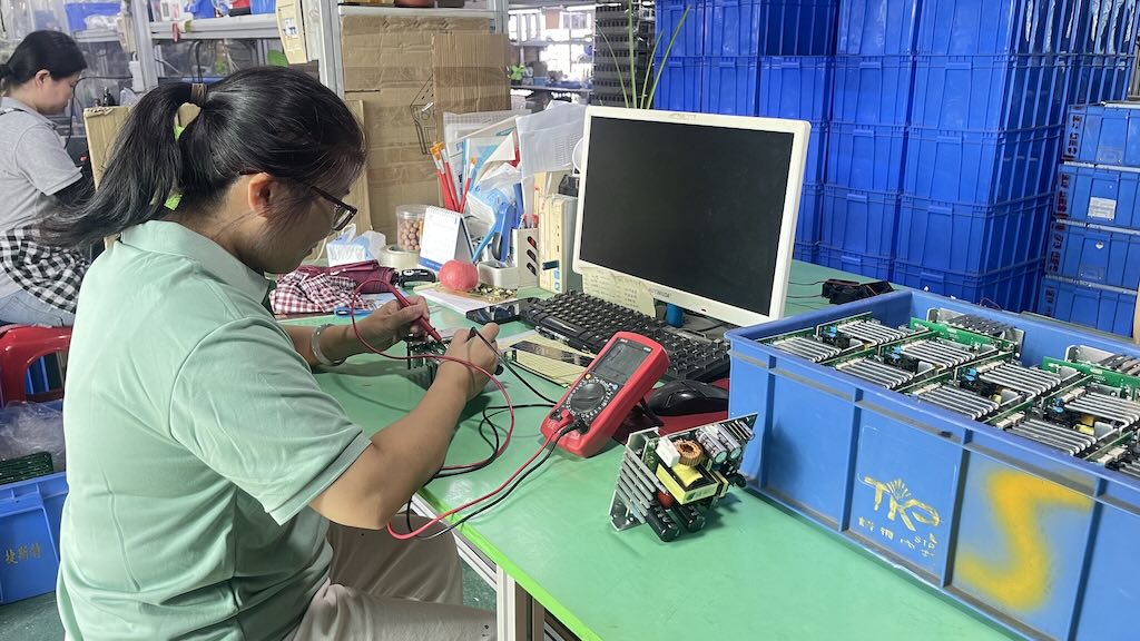 PCB Check
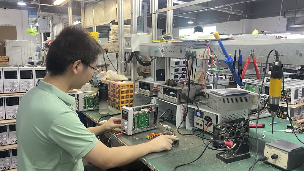 Debug
Debug
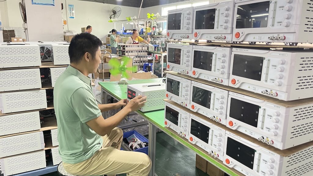 QC check
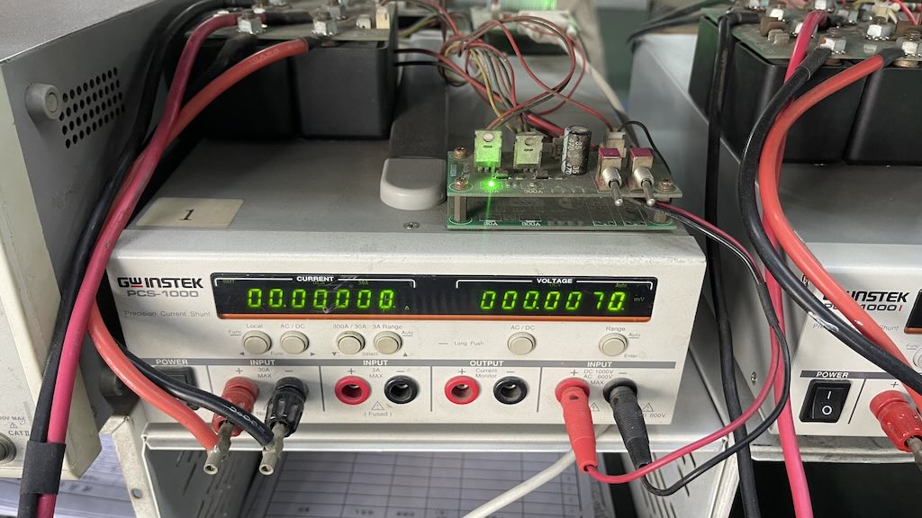 Multimeter
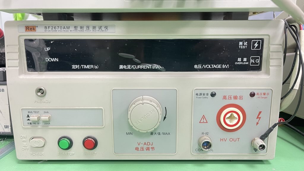 Hi-pot Tester
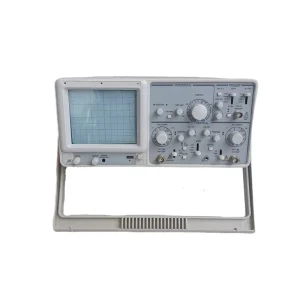
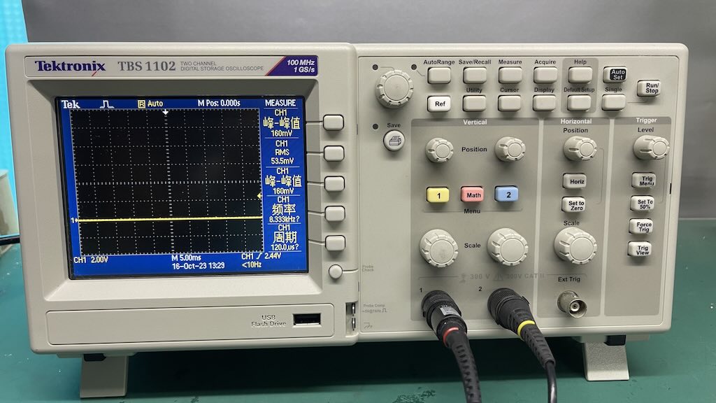 Oscilloscope
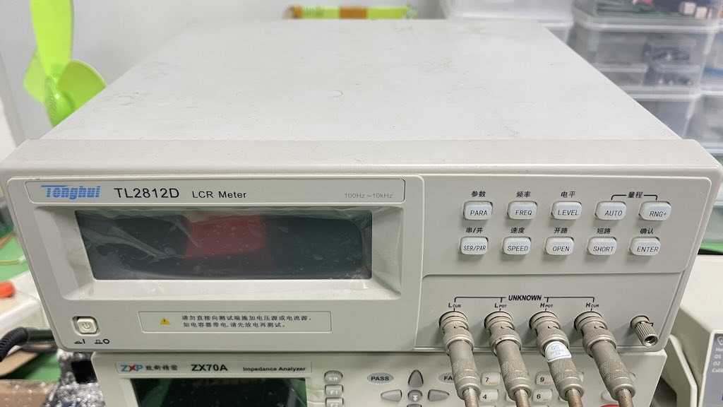 LCR Meter
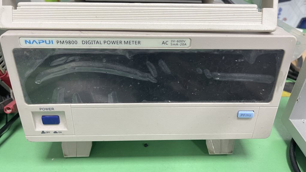 Digital power meter
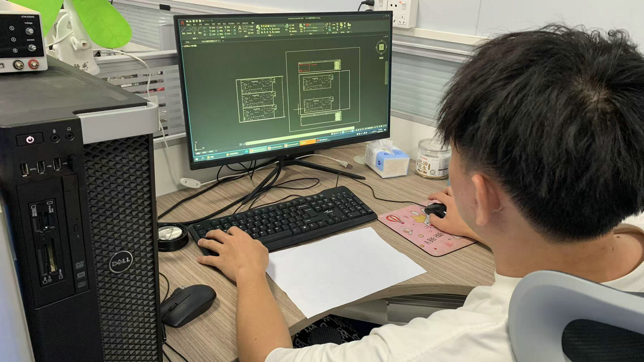 Design
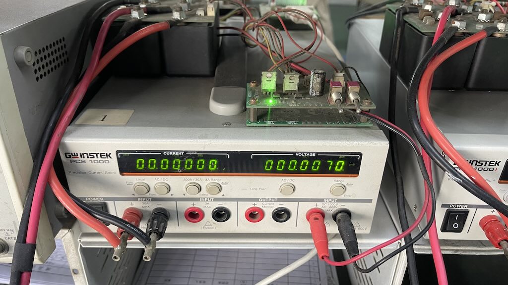 Multimeter
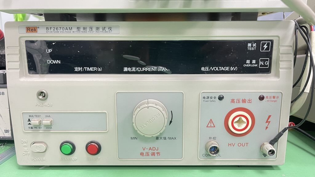 Hi-pot Tester
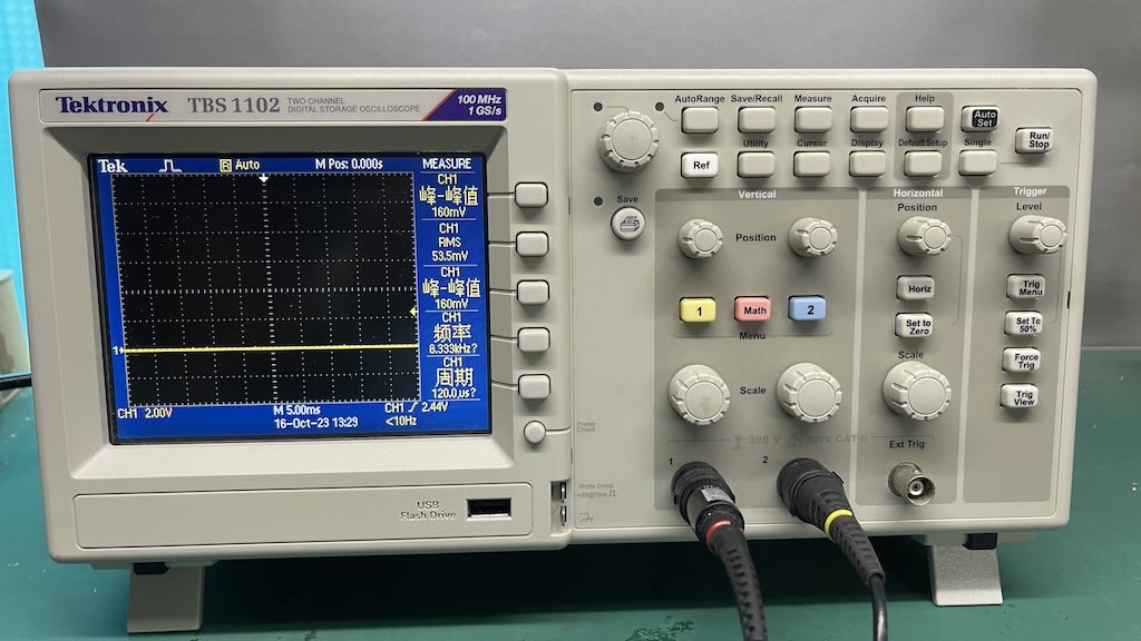 Oscilloscope
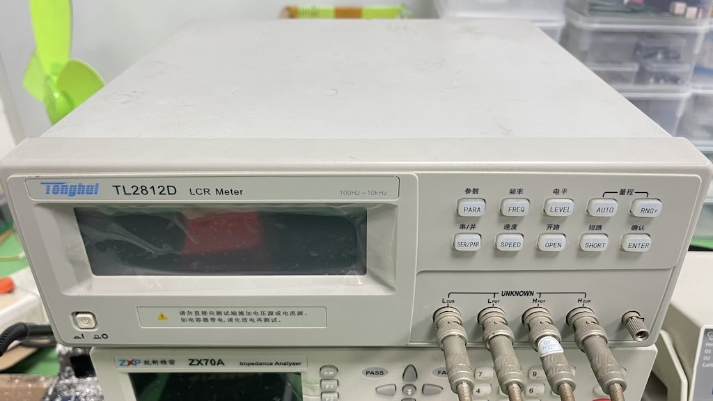 LCR Meter
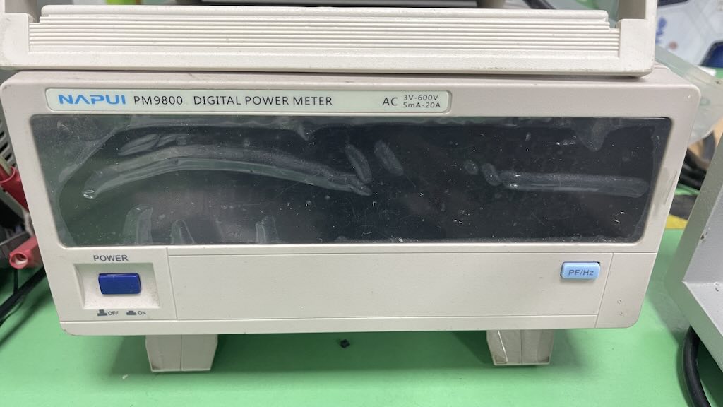 Digital power meter
Deploying specialized high-bandwidth and high-voltage differential probes in complex, real-world engineering environments.
In EV developments, measuring High-Voltage (HV) battery systems, motor control inverters, and On-Board Chargers (OBC) requires specialized differential probes. Engineers rely on high Common-Mode Rejection Ratio (CMRR) probes to separate tiny control signals from high-voltage noise switches (such as GaN and SiC MOSFETs) operating at potentials exceeding 800V.
With rise times dropping below 1 nanosecond in modern computing and IoT hardware, passive probes are highly susceptible to loading effects. Active probes with high input impedance (1MΩ to 10MΩ) and low input capacitance (<1pF) must be utilized to prevent altering the electrical characteristics of the signal path, ensuring accurate eye-diagram evaluations.
Avionics testing demands reliability under variable temperature ranges. Active probe designs must feature thermal stability compensation circuitry, preventing attenuation changes during environmental stress screening (ESS). CE certification acts as an essential quality gate to prevent electrical interference with critical communications equipment.
Adapting to Next-Generation Wide Bandgap Semiconductors, Optical Isolation, and Smart Automation
The fast-paced rise of Gallium Nitride (GaN) and Silicon Carbide (SiC) semiconductors has radically altered the requirements for test and measurement probes. Because wide bandgap devices switch in a matter of nanoseconds at high voltages, traditional passive and differential probes struggle to suppress parasitic oscillations and ground loops. The industry is rapidly shifting toward Optically Isolated Probing Systems.
By using optical fiber to transmit the measurement signal from the probe tip to the oscilloscope, complete galvanic isolation is achieved. This technology eliminates common-mode voltage limitations, providing near-perfect CMRR (up to 120dB at 100MHz). Additionally, future designs integrate auto-identification chips inside the BNC interface, allowing the oscilloscope to read attenuation ratios, calibration coefficients, and safety thresholds dynamically, eliminating manual configuration errors.
Assuring structural safety and system reliability under the EN 61010-031 testing framework.
To acquire the CE Certification, oscilloscope probes undergo rigorous laboratory evaluations. These tests analyze insulation material integrity, creepage distances, and clearance gaps between conductive channels. Furthermore, structural stress tests ensure that probe tips and leads do not snap or expose dangerous potentials during drops or heavy industrial handling. By adhering strictly to RoHS (Restriction of Hazardous Substances), MYAMI limits environmental footprint, ensuring all materials used are free from heavy metals such as lead, mercury, and cadmium.
Addressing the technical concerns of system engineers, calibration labs, and procurement agents.
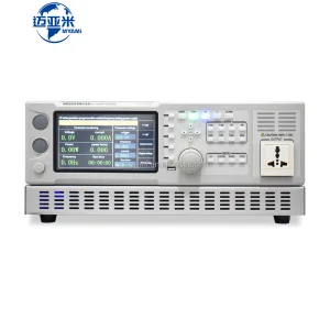
Select from our industry-grade benchtop devices, active/passive converters, and high-precision DC sources.

 Myami Power